Photonic microsystems "from Fab to Lab"
The Fraunhofer Institute for Photonic Microsystems IPMS is a leading international R&D service provider for electronic and photonic microsystems. Against this backdrop, researchers are also working on neuromorphic computing and various aspects of quantum technologies.

The cleanrooms at Fraunhofer IPMS are equipped to industry standards:
- 1,500 m² MEMS and MOEMS cleanroom (class 4 according to ISO 14644-1) – from process development to pilot production (200 mm)
- 300 m² microdisplay cleanroom (class 5 according to ISO 14644-1) – pilot line for microdisplays and sensors (200 mm)
- 2,700 m² CMOS cleanroom (class 6 and 3 according to ISO 14644-1) – development services on 300 mm wafers in the FEoL and BEoL areas for microelectronics
Extensive analysis and characterization tools round out the offering.
Through its research into key technologies, Fraunhofer IPMS promotes the development of independent and sustainable solutions that meet the requirements of the global market. The institute works closely with industry to drive innovation and ensure competitiveness.
Fraunhofer Institute for Photonic Microsystems IPMS, Dresden
Neuromorphic computing
Increasing digitalization is constantly driving up the demands placed on electronic hardware. Speed, performance, miniaturization, and energy efficiency are becoming increasingly important when it comes to enabling applications in the field of big data and artificial intelligence (AI).
A promising approach is offered by neuromorphic computing, which aims to replicate the self-organizing and self-learning nature of the brain. Fraunhofer IPMS develops materials, technologies, and complete hardware solutions with high energy efficiency, primarily for applications in the edge computing sector.
Technological developments are being pursued in various stages of expansion. Deep neural networks (DNNs) have already found their way into applications with the help of classic technologies (e.g., SRAM or flash-based) and initially mimic the parallelism and efficiency of the brain. Further miniaturization and reduction of energy consumption for edge applications is possible using new, innovative technologies. The next generation of so-called "spiking neural networks" (SNN) attempts to physically replicate the temporal component of the functionality of neurons and synapses, enabling even greater energy efficiency and plasticity. Here, too, innovative technology concepts are promising compared to classic technologies.
For both generations of neuromorphic hardware, Fraunhofer IPMS is researching crossbar architectures based on non-volatile memories, ferroelectric field-effect transistors. This is being done within various European (TEMPO, ANDANTE, STORAIGE) and Fraunhofer-internal funded projects. Particularly innovative materials research for future SNNs using Li-based systems is being conducted within the Saxon MEMION project.
Fraunhofer IPMS is working on new non-volatile memory technologies based on ferroelectric hafnium dioxide (HfO2) for analog and digital neuromorphic circuits. Ferroelectric materials are characterized by a change in their polarization when an electric field is applied. After the voltage is switched off, the polarization state is maintained. Using these ferroelectric field-effect transistors (FeFET) based on hafnium dioxide in 28- or 22-nm technology nodes, the weight values required for deep learning algorithms can not only be stored directly in the chip, but also calculated with them (so-called in-memory computing). Similar to the human brain, the hardware architecture of the chips is designed in such a way that information is already stored in the system and is non-volatile. There is no need for complicated data transfer between the processor and memory; the thinking power is already on the chip.
In contrast to the perovskite-based materials used to date, hafnium oxide-based memories are CMOS-compatible, lead-free, and scalable down to very small technology nodes. As the only non-volatile memory concept, ferroelectric memories are operated purely electrostatically and are therefore particularly energy-efficient, as only the recharge currents of the capacitors need to be used to write data. Memory and chip development is driven along the entire value chain, from applied materials research, component development, and integration architecture to IP generation and integrated systems.

IC design skills
The design of application-specific integrated circuits enables the production of highly complex microelectronic components such as microdisplays and optoelectronic sensors. The methodology of this design process is based on circuit simulation, layout design and verification. Fraunhofer IPMS in Dresden creates these designs using industry-standard software tools and implements them in mixed analog / digital CMOS processes in collaboration with silicon foundries worldwide. Once the circuits have been manufactured in silicon, the functionality is verified by tests at wafer and component level, after which prototypes are created. The transfer to pilot production can then take place on a project-specific basis.
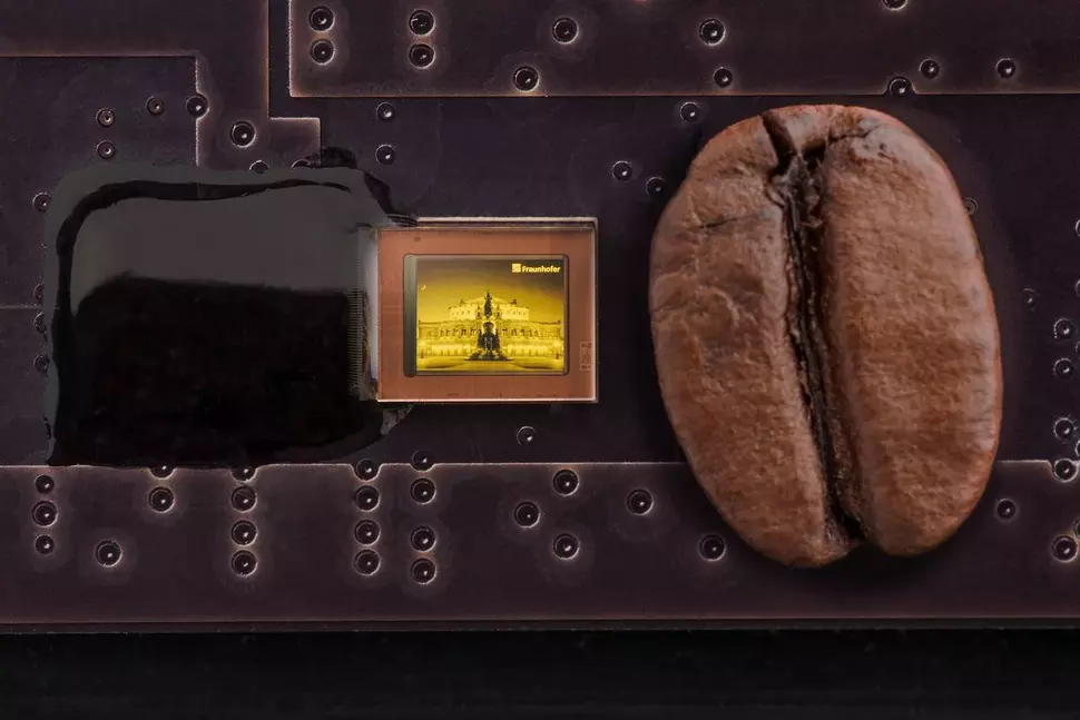
Fraunhofer IPMS occupies a unique position in the design of microelectronic circuits and components, as it makes application-specific and customer-specific adaptations to the CMOS processes of silicon circuit factories, which make it possible to subsequently apply OLED layers to the finished wafers, for example. This post-processing is used in particular to extend the functionality of silicon CMOS wafers with optical and photonic components, for example for high-resolution OLED microdisplays.
- Design of microelectronic circuits and modules through application-specific adaptation of CMOS processes
- Industry-compatible circuit simulation, layout design and verification
- Implementation in mixed analog/digital CMOS processes of silicon circuit factories
- Prototype production, transition to pilot production
Quantum technologies
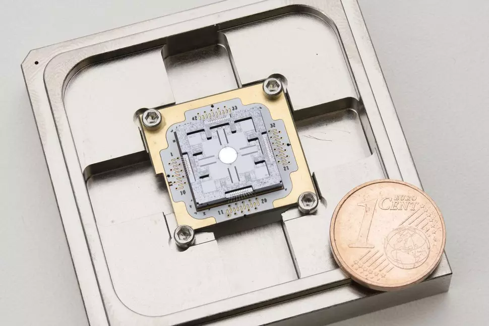
Fraunhofer IPMS conducts research into key components of quantum communication – from quantum key distribution (QKD) to quantum random number generation (QRNG) – and develops industry-oriented solutions that are suitable for both scientific collaborations and technology transfer projects.
Quantum computing "Made in Europe" – Fraunhofer IPMS conducts research on superconducting qubits, spin qubits, photon-based qubits, and neutral atom qubits. Fraunhofer IPMS is actively shaping the future of quantum technologies. Its work focuses on the development of scalable quantum computer hardware, ranging from materials research to industrial integration. With its 200 mm and 300 mm semiconductor manufacturing facilities, expertise in photonics, nanoelectronics, and microsystems technology, and close cooperation with industry partners, Fraunhofer IPMS bridges the gap between research and application.
Quantum Foundry "from Lab to Fab" – the basis for scalable quantum computers: Quantum manufacturing is a central building block for the technological sovereignty of Saxony, Germany, and Europe. Fraunhofer IPMS combines its expertise in micro and nanotechnologies, semiconductor processes, and assembly and connection technology to create the conditions for scalable quantum computers. At Fraunhofer IPMS, the focus is on the manufacturing implementation of qubits, the integration of control and readout systems, and material and process development. Cryogenics, precise measurement technology, and modular system architectures complement the research activities. This approach consistently implements the "from lab to fab" principle – from the laboratory to industrial production.
Quantum sensor technology is considered a key driver of innovation within modern quantum technologies. With CMOS-integrated NV sensors, Fraunhofer IPMS is developing a platform that enables highly sensitive quantum magnetometry at room temperature while leveraging the scalability, robustness, and energy efficiency of modern microelectronics. This combination of quantum metrology, photonics, and industrially compatible CMOS technology opens up new application prospects for research, medical technology, industry, energy infrastructure, and navigation.
Fraunhofer IPMS: Quantentechnologien