MICRO! - Research & Development

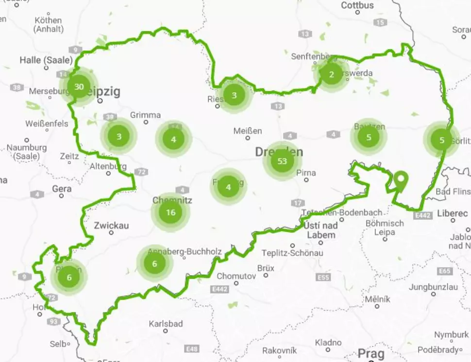
Saxony’s particular strong point is its very unique and compact research infrastructure. In the region, 4 Universities, 5 Universities of Applied Sciences, 9 Fraunhofer-, 3 Leibniz-, 1 Hemholtz- and 2 Max-Planck-Facilities are active in microelectronics / ICT research.

Im Rahmen des Exzellenzclusters „cfaed“ wird auch an der Echtzeit-Interaktion von Robotern und Menschen geforscht. „Versuchsobjekt“ ist ein gestengesteuerter NAO-Roboter (im Bild), der zukünftig zum Beispiel im Haushalt helfen könnte.

Source: Dresden University of Technology / cfaed / 5G Lab Germany, photo: Matthias Hahndorf

Cluster of Excellence „Center for Advancing Electronics Dresden (cfaed)“

The „Center for Advancing Electronics Dresden (cfaed)“ pools the research expertise of 60 scientists from the Dresden and Chemnitz Universities of Technology, as well as of 9 nonuniversity research institutes with the objective of researching entirely new technologies for the electronic information and data processing of the future in a globally unique, interdisciplinary approach. On the basis of novel materials – for example, silicon nanowires, carbon nanotubes, organic materials – new structural elements are being created which help construct innovative information processing systems.

"Tomahawk 2"-Mikrochip, entwickelt vom Vodafone Chair Mobile Communications Systems an der Technischen Universität Dresden

Source: Saxony Trade & Invest Corporation (WFS) / Jürgen Lösel

Vodafone Chair of Mobile Communications Systems, Dresden University of Technology

The Vodafone Chair of Mobile Communications Systems at Dresden University of Technology is the leading research institute for the mobile communication of the next generation (5G). Together with Vodafone, the Chair developed already the LTE successor; namely, “LTE Advanced.” The first transmitters were activated in 2013. In cooperation with Vodafone, it was possible to set a new world record (10.2 Gbit/s) in mobile data transmission outside the lab in 2015. Further industrial partners of the research team include such global players as, for example, Deutsche Telekom, National Instruments, Nokia, and Huawei. In order to develop 5G even further, the endowed chair founded the "5G Lab Germany" in which more than 600 scientists conduct research together. 

Nanoelectronic Materials Laboratory gGmbH (NaMLab), A Company of the Dresden University of Technology

The Nanoelectronic Materials Laboratory gGmbH (NaMLab) provides fundamental research in the materials science sector for nanoelectronic applications. One focus is on the analysis of materials for energy-efficient semiconductors. This also includes the integration of materials into new components and their electric characterization. 

Gedruckte Solarmodule, Institut für Print- und Medientechnik (IPM) der Technischen Universität Chemnitz

Quelle: Professorship Print Media Technology at the Chemnitz University of Technology (pmTUC) / Bystrik Trnovec

Institute for Print and Media Technology (IPM), Chemnitz University of Technology

The Institute for Print and Media Technology (IPM) at the Chemnitz University of Technology is a leading research institution in the printed functionalities and printed electronics sector. The researchers print transistors and batteries, loudspeakers and solar cells on flexible plastic foils or even paper – cost-efficient, color printable, and freely shapeable. The future fields of application are multifaceted – ranging from the „singing“ living room wallpaper to the time-saving „one-beep-registration“ of merchandise at the supermarket checkout via RFID labels all the way to „smart textiles“ which monitor the health status of the person wearing them.

Center for Microtechnologies (ZfM), Chemnitz University of Technology

The Center for Microtechnologies (ZfM) at the Chemnitz University of Technology has approximately 1,000 square meters of clean room space and is one of the best equipped university labs. The ZfM conducts research in the sector metallization systems for highly integrated circuits and the sector microsystems technology. It also produces prototypes and pilot series and develops innovative procedures and materials. 

Dresden Integrated Center for Applied Physics and Photonic Materials (IAPP), Dresden University of Technology

The Dresden Integrated Center for Applied Physics and Photonic Materials (IAPP) at the Dresden University of Technology has extensive expertise in the analysis of physical properties of organic materials and their application in such components as OLEDs, solar cells and switching components. A special research focus is on the doping of highly efficient organic components with the help of doped molecular materials. This has allowed the institute to actually earn several world records in the efficiency of OLEDs and organic solar cells. 

Dresden Center for Nanoanalysis (DCN), Dresden UNiversity of Technology

In April 2013, the Dresden Center for Nanoanalysis (DCN) was officially opened in cooperation with the Cluster of Excellence „Center for Advancing Electronics Dresden (cfaed)" at Dresden UNiversity of Technology. The DCN’s core competences include the development of imaging methods for surveying and recording kinetic processes in the nanometer range. Towards this end, the smallest possible structures are investigated with a resolution at the atomic level in order to characterize new materials, processes, and structural elements. 

Freiberg University of Mining and Technology

As an acknowledged and renowned „university of resources,“ the Freiberg University of Mining and Technology primarily addresses topics which revolve around materials and raw materials for the semiconductor industry. One of its latest research highlights is a new process for the recycling of rare earths from old smartphones, extinguished neon tubes, or discarded computer monitors which the Freiberg University of Mining and Technology has developed together with the FNE Entsorgungsdienste Freiberg GmbH and NARVA Lichtquellen GmbH & Co. KG corporations. 

Bidirektionaler SVGA-OLED-Mikrodisplay, Fraunhofer-Institut für Organische Elektronik, Elektronenstrahl- und Plasmatechnik FEP, Dresden

Source: Fraunhofer Institute for Organic Electronics, Electron Beam and Plasma Technology FEP / Jürgen Lösel

Fraunhofer Institute for Organic Electronics, Electron Beam and Plasma Technology FEP, Dresden

The Fraunhofer Institute for Organic Electronics, Electron Beam and Plasma Technology FEP in Dresden conducts work on vacuum coating and surface treatments, and is Europe’s leading center for research on and the pilot production of devices and manufacturing technologies based on organic semiconductor materials. The core competencies of the institute consist of electron beam technology, sputtering, plasma-activated high-rate deposition, high-rate PECVD, technologies for organic electronics and IC / system design. It offers a broad spectrum for research, development and pilot production for the treatment, sterilization, structuring and finishing of surfaces as well as for OLED micro-displays (combination of silicon micro-electronics and organic electronics), sensors, optical filters and flexible OLED lighting. 

Die vom Fraunhofer-Zentrum THM gemeinsam mit Partnern entwickelte neue HVPE-Anlage ist seit Anfang 2014 in Freiberg in Betrieb und stellt bei guter Materialqualität sowohl transparente GaN-Schichten als auch GaN-Kristalle mit Dicken im mm-Bereich her.

Source: Fraunhofer Technology Center for Semiconductor Materials THM, Freiberg

Fraunhofer Technology Center for Semiconductor Materials THM, Freiberg

The research conducted at the Fraunhofer Technology Center for Semiconductor Materials THM in Freiberg focuses, on the one hand, on decreasing the production costs of semiconductor substrates and developing innovative energy storage and energy conversion materials. In cooperation with the Freiberger Compound Materials GmbH (FCM), the 25 institute has developed a new plant concept which significantly lowers the production costs of the important semiconductor material gallium nitride (GaN), for example, by using materials which reduce wear and tear as well as innovative process measurement technologies. 

Fraunhofer Institute for Photonic Microsystems IPMS, Dresden

The Fraunhofer Institute for Photonic Microsystems IPMS in Dresden is one of the pioneers of MEMS development worldwide. The institute researches in electronic, mechanical and optical components and their integration into miniature „intelligent“ devices and systems. The institute’s specific competence is in the use of light for various purposes, i.e. the application of optical properties and components. The integrated Center for Nanoelectronic Technologies CNT carries out industry-related research into 300-mm wafers for semiconductor manufacturers and their suppliers. Together with three other Fraunhofer Institutions and the Dresden and Chemnitz Universities of Technology, IPMS forms the „Functional integration for micro- and nanoelectronics“ performance center. This is where development is undertaken on, for example, sensor nodes for networked systems, adaptive diagnostic systems and control systems designed to minimize the energy consumption in production. On completion of the pilot phase, the focus will then turn to the areas of energy and medical technology as well as mobility. 

Fraunhofer Institute for Electronic Nano Systems ENAS, Chemnitz

The research and development activities of the Chemnitz-based Fraunhofer Institute for Electronic Nano Systems ENAS focus on smart systems using micro and nano technologies. These intelligent systems not only integrate components of differing functionalities, but are also able to record and recognize complex situations. They can make decisions, interact with the environment as well as function on an energy-autonomous and networked basis. The institute’s portfolio ranges from highprecision sensors for industry, sensor and actuator systems with control and evaluation electronics to such printed functionalities as antennas or batteries all the way to materials and reliability research for microelectronics and microsystems technology. 

MEMS-Lautsprecher, Fraunhofer-Institut für Elektronische Nanosysteme ENAS, Chemnitz

Source: Fraunhofer Institute for Electronic Nano Systems ENAS, Chemnitz

Fraunhofer IZM – All Silicon System Integration Dresden ASSID

The Fraunhofer IZM – All Silicon System Integration Dresden ASSID develops wafer level packaging and system integration technologies for 3D integration and transfers these technologies into products. The institute possesses a complete 200-mm / 300-mm process line for 3D wafer level system integration based on the copper-through-silicon-via (Cu- TSV) technology. The service spectrum of the Fraunhofer IZM-ASSID encompasses customer-specific developments and prototyping as well as mass production in small batches and technological process transfer. 

Helmholtz Center Dresden-Rossendorf e. V. (HZDR)

The Helmholtz Center Dresden-Rossendorf e. V. (HZDR) develops innovative materials for the computer technologies and storage systems of tomorrow. The Ion Beam Center and its broad range of methods for the analysis and treatment of surfaces is also available to semiconductor firms. In order to improve the quality of monocrystals, the HZDR researchers calculate the magnetic fields which are required to produce perfect wafers with diameters of 300 mm and/or 450 mm from liquid, molten silicon. 

Together with the Freiberg University of Mining and Technology, the HZDR operates the Helmholtz Institute Freiberg for Resource Technology (HIF) with the objective of developing new technologies for providing and utilizing mineral and metalliferous raw materials more efficiently, and for recycling these resources in an environmentally friendly manner. 

Together with the HIF, the HZDR coordinates the establishment of Europe’s largest resource network. Until 2022, a total of 410 million euros will be available for „EIT RawMaterials“ with the objective of developing new procedures and products for the sustainable exploration, extraction, processing, and recycling of raw materials.

Fraunhofer Institute for Ceramic Technologies and Systems IKTS, Dresden

The Fraunhofer Institute for Ceramic Technologies and Systems IKTS in Dresden, develops measurement and testing technologies for electronics, microsystems technology, and nanotechnology as well as electronics and sensor technology for measurement and testing systems. The service portfolio includes software development, simulation, and testing services. 

Social Media

Top